Sub Micron Bonding Solutions for Opto-electronic Packaging
...at LASER WORLD of PHOTONICS Hall B3 booth 359.
Today's advanced packaging and bonding technologies for opto-electronic and photonic applications are characterized by rapid transformation and ever-more specific demands regarding the assembly equipment. When investing in a machine solution, it's not only about the specs. Equally important is to rely on a solution which promises maximum technological flexibility, compatibility with future technologies, adaptability, longevity, as well as all-around economics.
With an industry-leading product line-up ranging from manual to fully-automated sub-micron bonding systems, German manufacturer Finetech offers equipment for high-precision die packaging and assembly challenges that can do just that. In the spirit of true developer's platforms, all FINEPLACER® sub-micron bonders can be configured to provide optimal process environments for each application. Their modular system architecture allows highly-individualized machine configurations. Instead of acquiring another machine, new processes and technologies can be added by retrofitting the system with extension modules. Intelligent and customizable interface solutions allow integrating various upstream or downstream processes such as optical facet inspection or the implementation of measuring equipment. This makes a FINEPLACER® system a long-standing and future-proof investment. Each FINEPLACER® system has been 100% designed and manufactured in Germany, with highest production standards being guaranteed through an ISO 9001 certified quality management.
FINEPLACER® sub micron systems mainly vary in their degree of automation, their optical resolution and their capability to handle substrates and components of various sizes. Below is a selection of FINEPLACER® bonding systems particularly suitable for the specifics of opto-electronic and photonic applications. Alternative systems with other specifications in terms of supported substrate and component dimensions as well as configuration options are available.
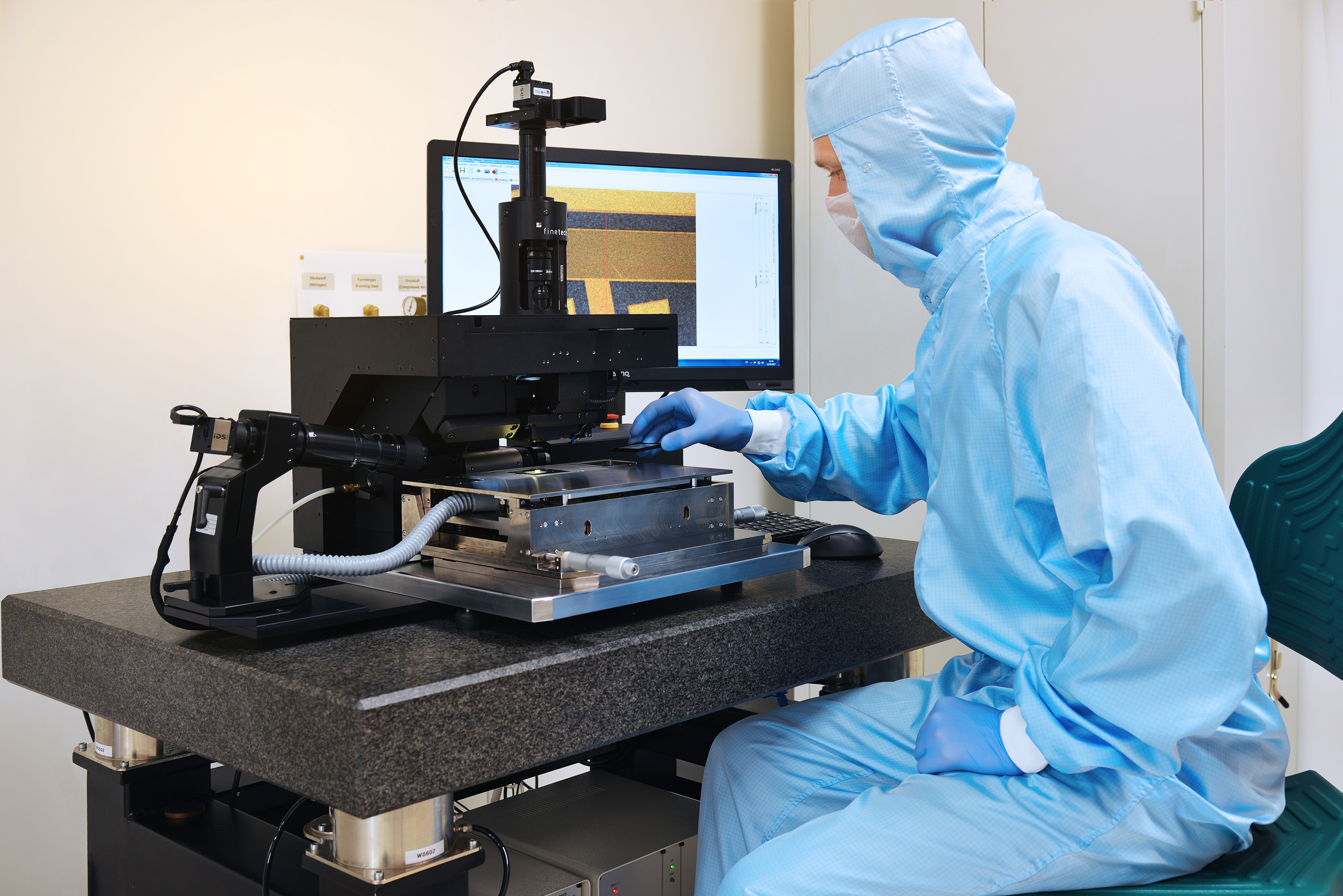
FINEPLACER® lambda – Superior resolution and technological flexibility
The acclaimed sub-micron Opto-Bonder® FINEPLACER® lambda offers outstanding optical resolution and can be easily reconfigured for precision die attach and advanced packaging in photonics and opto-electronic applications. Available in manual or motorized configurations, the device is the premier choice when maximum technological versatility and fast process implementation is key. Typical fields of application include R&D, universities, prototyping and low-volume production. The system is capable of handling component sizes from 0.07 x 0.07 mm² to 60 x 90 mm² on a working area up to 190 mm x 52 mm. Wafer sizes up to 6'' are supported. A wide range of applications can be handled, including laser bar and diode bonding with Indium or Au/Sn, VCSEL/photo diode bonding (glueing, curing), the assembly of lenses, mirrors or filters, and the multi-stage assembly of opto electro mechanical systems (i.e. MEMS/MOEMS) for communications and medical technology products.
FINEPLACER® femto - Fully-automated sub-micron bonding with high yield
The FINEPLACER® femto is a fully automated platform for advanced flip chip bonding and die attach applications. The Vision Alignment System is combined with pattern recognition for high-precision automatic alignment and sub-micron bonding results. This field approved system offers modular application architecture and can be flexibly equipped for a wide range of die bonding applications and processes. It is an ideal system for product and process development as well as production environments especially in the opto-electronic sector. The platform is capable of accommodating the complete production workflow of inspection, characterization, packaging, final test and qualification. With unrivaled versatility and excellent cost-performance-ratio, the FINEPLACER® femto is truly setting standards in its class.
Finetech – More than Machines
In the quest to find the best answer to an application challenge, the FINEPLACER® system is only one part of the solution. Finetech co-operates closely with the customers to ensure that all aspects and requirements of a challenge are tackled. With a state-of-the-art production and development center in Berlin, Finetech is well-positioned to provide comprehensive application solutions enhanced with cleanroom application tests, process development support as well as in-depth technology consultation, customer training and various other services. Finetech also maintains a world-wide network of representatives as well as direct sales & service centers in the US, China, Japan and Malaysia to guarantee quick response times, local support and on-site presence in global key markets.
Finetech is exhibiting at Laser World of Photonics Hall B3 booth 359.