Advanced Sub Micron Bonder
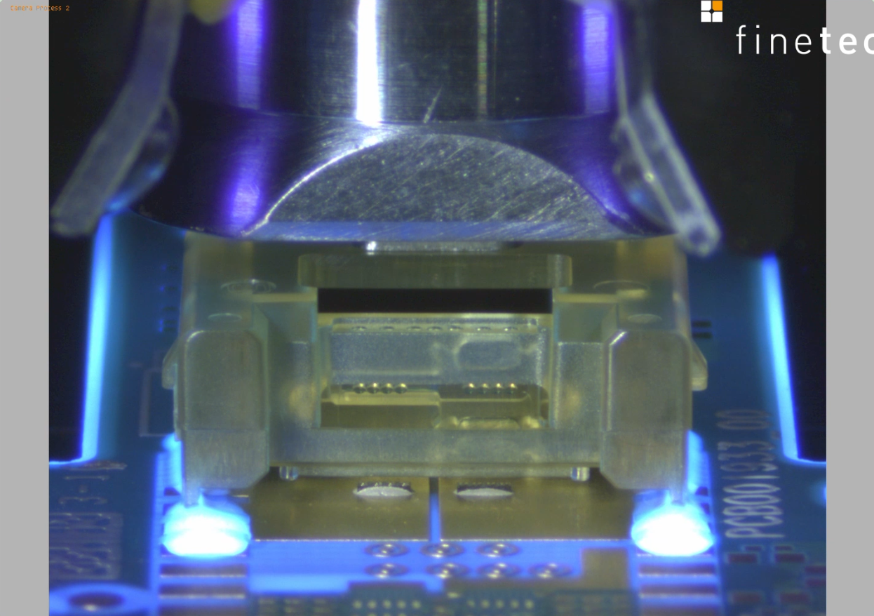
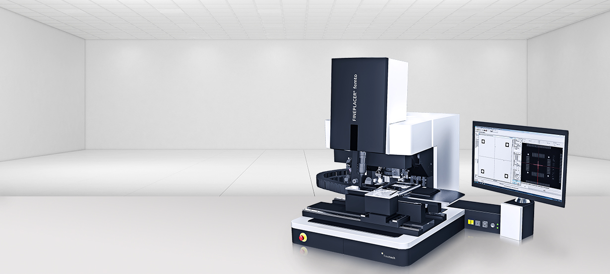
The FINEPLACER® femto is a fully automated, sub-micron bonding platform for advanced flip chip bonding and die attach applications. The Vision Alignment System is combined with automatic pattern recognition for high-precision alignment and sub-micron bonding results.
This field approved system offers modular application architecture and can be flexibly equipped for a wide range of die bonding applications and processes. It is an ideal system for product and process development as well as production environments in the opto-electronics sector. The platform is capable of accommodating the complete production workflow of inspection, characterization, packaging, final test and qualification.
FINEPLACER® femto has the best cost - performance ratio of its class in the market.

Key Facts*
- Numerous bonding technologies (adhesive, soldering, thermocompression, ultrasonic)
- Reproducible highest placement accuracy
- Ultra low bonding force
- Operating software with full process access and easy programming
- Fully automatic and manual operation
- Quick setup of new applications
- Full process traceability and protocol function incl. photo and video capturing
- Plug & Play configuration of process modules
- Synchronized control of all process related parameters: force, temperature, time, power, process environment, light, vision
- Overlay vision alignment system (VAS) with fixed beam splitter
- In-situ process observation in HD
- Data/media logging and reporting function
- Modular machine platform allows in-field retrofitting
- Small footprint, compact design
Applications & Technologies
With a broad range of supported applications and technologies, our die bonding systems are ready to tackle any application challenge in the industry. And as market requirements shift and new technologies emerge, their modular hardware and software architecture ensures maximum technological versatility over the entire service life.
Functions - Modules - Enhancements
Our die bonding solutions are as individual as our customers' requirements and offer a wide range of configuration options. In addition to the system's basic functions, which are part of the standard functional range, numerous process modules are available for each system, expanding the spectrum of applications. Retrofittable at any time, they enable additional die bonding technologies and processes either directly or as part of a module package. A selection of functional enhancements and accessory systems make daily work with the die bonder easier and help to make certain technology and process sequences even more efficient.
Motorized dipping unit for viscous materials like flux or adhesives. Suitable for use with stamping tools or for direct dipping of various sized components. Adjustable for dipping baths with different thicknesses.
Enhances the existing bond force range and allows the use of software controlled process forces.
Direct contact heating from the top with chip specific tool design to apply temperature from the chip side. E.g. used for thermocompression, gluing or ACA bonding
Allows presentation of components via Gel-Pak®, VR trays, waffle packs or tape holders as well as the support of dipping trays.
Allows flipping of components prior to face-down assembly.
Integration of dispensing systems for applying adhesive, flux, solder paste or other pasty material. Various supported types like time-pressure, volume and jet dispensers.
Together with the main camera, the additional camera allows two object field sizes without zoom or different object field positions. Improves the display of large objects and thus accelerates the workflow.
The “Known Good Die" testing allows chip probing / testing prior to the bonding process.
Creates an inert or reactive (CH2O2) process atmosphere. Used to reduce and prevent oxidation during soldering (e.g. eutectic or indium bonding). Add-on for Substrate Heating Modules.
Used to handle and rotate substrates up to 360° independently from the bonding tool.
Allows automatic focus setting of component and substrate as well as height measurements.
Manual squeegee units for viscous materials like adhesives or flux. Suitable for use with stamping tools or for direct dipping of various sized components. With adaptable layer thicknesses.
Allows to adjust different camera positions along the x-axis of the system. Useful to align large components with maximum magnification.
Precise visual alignment of chip and substrate.
Controls an inert or reactive (H2N2) atmosphere in an enclosure or with the bond head. Used to prevent or reduce oxidation during soldering or bonding.
Allows the in-situ observation of the working area during the bonding process.
Improve the wetting condition of bonding surfaces and reduces voids. Oxide layers are scrubbed off in a low frequency mechanical sonic process.
Various direct contact heating options to heat up substrates from the bottom during the process. Substrate-specific fixations available. Optionally with process gas integration. Used e.g. for thermocompression, thermal adhesive or thermosonic bonding.
Unheated support plate with substrate specific fixation (e.g. vacuum) to clamp various substrates.
A small red point accelerates the working flow | Enables coarse position alignment of the table to the tool with the help of a laser spot.
Automatic tracking and logging of all process relevant parameters (e.g. temperature, force, etc.) as well as associated component details (e.g. serial numbers).
Enables ultrasonic or thermosonic bonding. Transmits mechanical energy based on lateral movement of the ultrasonic transducer to the component while it is in contact with the substrate.
Provides ultra violet LED-light in various wave lengths for adhesive processes without thermal influence. The UV source can be attached to the tool or mounted to the substrate holder.
Special substrate heating module designed for large wafers. Very uniform heat distribution during chip to wafer or wafer to wafer bonding.
Allows the adaptation of the Vision Alignment System for an optimized view of components and substrates.
Technical Papers

Laser Bar Bonding
Semiconductor Laser diode bars are high power products, used in places where small and efficient emitting light sources are needed. Primarily, these Lasers are being used as pumping sources for optical resonators of solid state Lasers or gas Lasers.